The National Aeronautics and Space Administration (NASA) Engineering and Safety Center (NESC), operating out of the Langley Research Center in Hampton, Virginia, has published a critical technical bulletin addressing an unusual and high-risk hardware failure mode in aerospace electronics. Authored by Meagan Chappell with oversight from contact official Joel W. Sills, the advisory—designated as Technical Bulletin TB-26-10—details the unexpected transverse cracking of alumina substrates in thick-film chip resistors during standard environmental acceptance testing. Although thick-film chip resistors are ubiquitous components utilized across virtually all modern NASA flight hardware, deep-space probes, and orbital platforms, instances of alumina substrate cracking during testing remain exceptionally rare.
The publication of this bulletin follows a thorough independent engineering investigation into two distinct failure events observed on printed circuit board assemblies. The findings offer immediate mitigation strategies, manufacturing design considerations, and assembly guidelines for aerospace contractors, prime system developers, and component engineers striving to eliminate structural vulnerabilities in critical ceramic body components.
Chronology and Background of the Failures
The sequence of events leading to the publication of Technical Bulletin TB-26-10 began during routine environmental acceptance testing of mission-critical printed circuit board assemblies. The hardware in question underwent standard qualification screening, which sequentially paired vibration testing with subsequent thermal cycling protocols.
During the thermal cycling phase—designed to precipitate latent manufacturing defects and stress concentrations by subjecting assemblies to severe temperature fluctuations—operators noted intermittent open-circuit electrical failures. Significantly, these electrical faults exhibited a thermal dependency: the circuits failed during high-temperature dwell periods but mysteriously recovered their electrical continuity as the assemblies returned to room temperature. This thermal expansion and contraction behavior strongly indicated a mechanically induced fracture that opened under thermal stress and closed when thermal contraction brought the severed faces back into physical contact.
Subsequent physical inspection of the two affected assemblies revealed a striking pattern. In both instances, the failures occurred in identical thick-film chip resistors mounted in nearly identical physical locations near the outermost edges of the printed circuit boards. Upon microscopic examination, engineers discovered that both components had suffered a severe structural fracture across their short axes, running precisely parallel to the metallic terminations at the mid-span of each resistor body.
Because both failed resistors originated from the same production lot, initial engineering theories naturally gravitated toward a hypothesis of batch-level manufacturing defects or vibration-induced cyclic fatigue. However, rigorous analytical protocols quickly challenged these preliminary assumptions, setting off a multi-agency engineering review to uncover the true root causes of the structural degradation.
Rigorous Failure Analyses and Elimination of Preliminary Theories
To diagnose the underlying mechanics of the fractures, the NESC initiated comprehensive, independent failure analyses involving advanced optical microscopy and scanning electron microscopy (SEM).
Initial suspicions focused heavily on the possibility that the components suffered from latent structural flaws introduced during fabrication by the manufacturer. To test this hypothesis, engineers evaluated the procurement documentation and compliance metrics for the affected components. The resistors were certified under military specification MIL-PRF-55342, a rigorous standard governing fixed-film chip resistors for high-reliability space applications. Furthermore, quality assurance teams pulled unmounted samples from the identical production lot and subjected them to destructive and non-destructive screening. The testing yielded no evidence of elevated defect rates, material inhomogeneities, or structural weakness within the production lot, effectively clearing the component manufacturer of supplying sub-standard hardware.
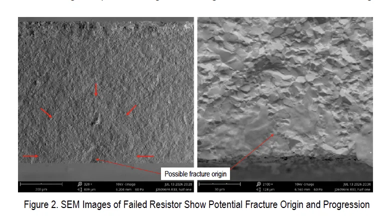
Researchers then investigated whether vibration-induced cyclic fatigue could have initiated and propagated the cracks during the vibration testing phase. During launch and routine spacecraft maneuvers, circuit boards experience intense random vibration profiles that induce high-cycle mechanical stress. However, detailed fractographic analysis using SEM imaging revealed no classic signatures of fatigue crack progression, such as striations or beach marks. Instead, the fracture surfaces displayed clean, single-plane tensile breaks running directly across the short axis of the ceramic body.
Furthermore, the absence of any twisting or out-of-plane shear deformation ruled out complex multi-axial twisting forces. The damage morphology pointed conclusively to a pure bending or tensile overstress event, wherein mechanical deflection of the underlying printed circuit board placed the brittle ceramic substrate under excessive tensile stress until it snapped.
Contributing Factors and Systemic Implications
With material flaws and vibration fatigue effectively ruled out, the NESC inquiry shifted its focus to the mechanical interaction between the printed circuit board substrate, the mounting solder joints, and the rigid ceramic chip components. Although no single root cause could be assigned to a specific manufacturing error, the investigation successfully isolated a constellation of compounding factors that dramatically increase the risk of flexure-induced cracking in large-footprint ceramic components.
Foremost among these contributing factors is board flexure. During manufacturing, depanelization, component insertion, connector mating, and mechanical fastening, printed circuit boards routinely experience physical bow and twist. When a circuit board flexes, rigid surface-mount components—particularly those featuring brittle ceramic substrates like alumina ($textAl_2textO_3$)—must accommodate the strain of the bending substrate.
Component orientation and location emerged as critical exacerbating variables. Both failed resistors were large-footprint devices situated in close proximity to the mechanical edges of the printed circuit boards. Board edges are well-documented zones of heightened mechanical stress during handling, thermal expansion mismatches, and chassis installation. When a large ceramic component is oriented in a manner that forces its long axis to align with primary board deflection vectors, the component acts as a stiffening bridge, absorbing disproportionate amounts of mechanical strain.
Additionally, the investigation scrutinized soldering practices. Excessively high solder fillets can anchor the ceramic body too rigidly to the board pads, restricting the natural micro-flexure allowed by compliant solder joints and transmitting board-level strains directly into the brittle ceramic core. When combined with the thermal stresses of subsequent environmental testing, these accumulated installation and manufacturing loads easily exceed the ultimate tensile strength of the alumina material, culminating in catastrophic transverse cracking.
Official NESC Recommendations and Assembly Guidelines
To prevent similar failures in future spaceflight hardware and high-reliability commercial applications, the NESC Technical Bulletin outlines a stringent framework of engineering and manufacturing guidelines. These recommendations are designed to bridge the gap between mechanical design, circuit board layout, and environmental testing protocols:
-
Careful Component Placement: Design engineers must strategically position large-footprint ceramic body components away from high-stress areas, specifically avoiding the immediate perimeters, edges, and connector mounting zones of printed circuit boards where board bow and twist are most pronounced during handling and assembly.
-
Finite Element Analysis (FEA): Project teams are strongly encouraged to employ advanced finite element modeling early in the design phase to simulate board-level mechanical behavior during thermal cycling and vibration. FEA models can accurately predict high-stress regions and guide layout adjustments before physical hardware is fabricated.
-
Controlled Solder Fillet Height: Manufacturing processes must maintain strict oversight of solder volume. Automated optical inspection (AOI) and visual standards should be implemented to ensure that solder fillet heights do not become excessive, thereby preventing the rigid locking of ceramic components to the substrate pads and allowing for necessary mechanical compliance.
-
Thorough Manufacturing Inspection: Quality control protocols must incorporate enhanced inspection techniques—such as high-magnification optical screening and X-ray inspection—to detect pre-existing micro-cracks, handling damage, or board warpage prior to environmental acceptance testing.
-
Functional Thermal Shock and Burn-In Testing: To identify latent mechanical instabilities before hardware integration, test engineers should utilize targeted thermal shock and thermal cycling profiles combined with continuous in-situ electrical monitoring to catch intermittent open-circuit anomalies that might otherwise recover at ambient laboratory temperatures.
Broader Industry Impact and Standards Reference
The release of Technical Bulletin TB-26-10 underscores the relentless pursuit of zero-defect reliability required in modern aerospace engineering. While thick-film chip resistors have maintained an exemplary service history across decades of space exploration, the increasing miniaturization of electronics, coupled with the deployment of larger component footprints on increasingly dense printed circuit boards, introduces subtle mechanical failure modes that traditional electrical testing alone cannot predict.
By formalizing these lessons learned, NASA aims to protect upcoming robotic missions, crewed spacecraft, and orbital observatories from unexpected electrical failures driven by mechanical stress. Industry primes, subcontractors, and electronics manufacturers are expected to review their current design rule decks against the new NESC guidelines, ensuring that printed circuit board layout practices adequately account for the mechanical fragility of ceramic substrates.
For further technical inquiries, documentation, and access to the complete advisory, aerospace professionals and researchers are encouraged to contact Joel W. Sills at the NASA Langley Research Center via email at [email protected], or consult the official technical publication index under reference designations MIL-PRF-55342 (covering established and non-established reliability fixed film chip resistors for space applications), MIL-PRF-55342/9 (specifically governing style RM2512 components), and MIL-STD-202 Method 218 (outlining standard board flexure test methods).